Underfill Materials for Flip-Chip & BGA Packaging
Reinforcement and stress relief for advanced semiconductor packaging.
Ideal for flip-chip, BGA, and high-reliability applications in microelectronics.
Stress-Relief and Reinforcement for Flip-Chip and BGA Assemblies
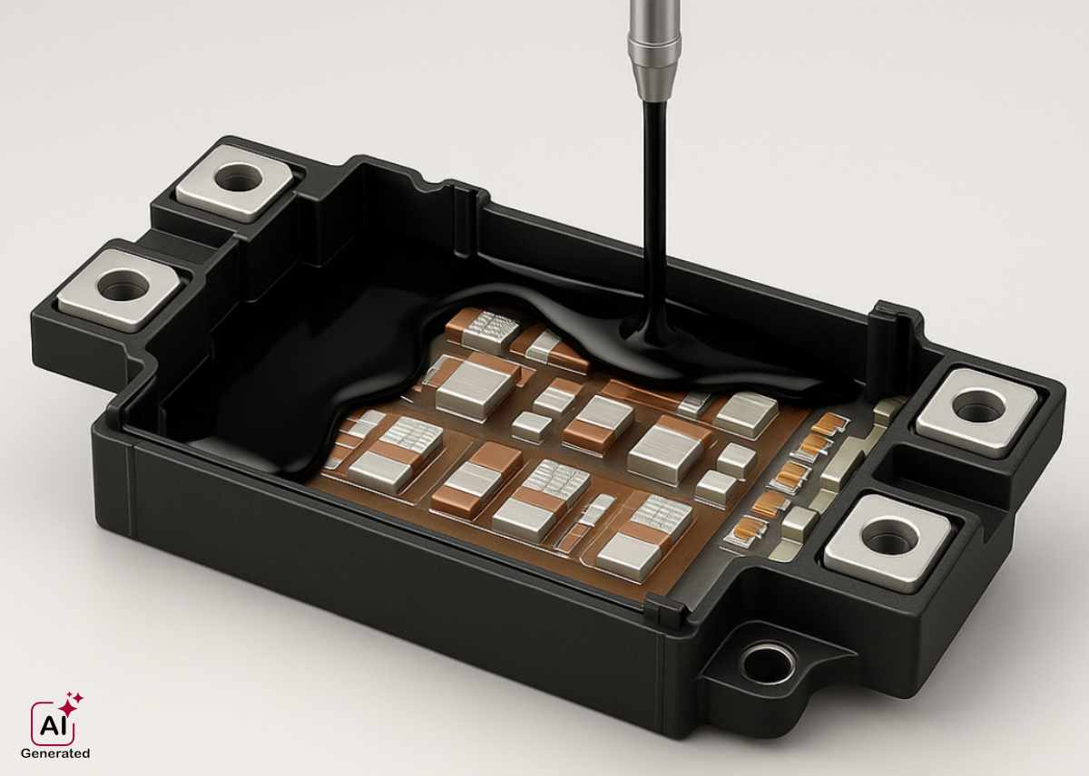
Underfill materials are specialty resins used in flip-chip, BGA, and CSP packaging to enhance mechanical stability, thermal cycling resistance, and long-term reliability. By filling the gap between die and substrate, underfill absorbs stress from thermal expansion mismatch and protects solder joints from fatigue and failure.
These materials are essential for mobile devices, automotive electronics, sensors, MEMS, and power semiconductors operating under demanding conditions.
NAGASE provides high-performance underfill solutions tailored to advanced semiconductor packaging requirements worldwide.
Applications
Underfill materials are used to improve reliability in microelectronic assemblies by reinforcing interconnects and protecting solder joints.
- Flip-chip encapsulation for ICs and SoCs
- BGA and CSP packaging reinforcement
- Underfill for MEMS and sensor modules
- Stress relief in power semiconductor packaging
- Mobile, automotive, and high-reliability electronics
Features
NAGASE’s underfill materials ensure mechanical stability, thermal durability, and excellent wetting for reliable flip-chip and BGA performance.
- High adhesion strength – Protects solder joints under thermal stress
- Low thermal expansion – Reduces mechanical strain during temperature cycling
- Fast flow and good wettability – Ensures complete capillary filling
- Compatible with lead-free and fine-pitch packages
- Customizable properties – Viscosity, cure speed, filler content, and more
Additional Information
- Good flowability for narrow gaps
- High adhesion to various surfaces
- Flux compatibility
- Meets the requirements of RoHS and EU REACH


