
Tetraethyl Orthosilicate for Precision CVD and Thin Film Deposition
Reliable performance for next-generation semiconductor fabrication.
Nagase’s high-purity TEOS ensures optimal film quality, consistency, and reliability across a wide range of deposition environments.
High-Purity TEOS for Advanced CVD and Oxide Layer Fabrication
Tetraethyl orthosilicate (TEOS) is a high-purity silicon compound used as a key precursor in chemical vapor deposition (CVD) for producing high-quality silicon dioxide (SiO₂) films. It plays a crucial role in forming uniform insulating layers on semiconductor wafers and is valued for its excellent volatility, reactivity, and process control. TEOS is widely used in microelectronics, photonics, and MEMS fabrication where precise dielectric properties are essential.
As a trusted supplier for the electronics industry, NAGASE offers ultra-high purity TEOS optimized for cleanroom environments, ensuring consistent quality, stable film growth, and low defect levels.
Chemical Formula: Si(C2H5O)4
Molecular Weight: 208.33
Physical & Chemical Properties:
Appearance: apparently colorless liquid
Melting point: -77 ℃
Boiling point: 169 ℃
Relative density: 0.9346 g/ml
Stable in air. Slightly soluble in water. Hydrolyze very slowly in pure water. Acid or base can speed up its hydrolyzation.
Applications
Application Areas
TEOS is widely used in advanced material processing where precise oxide film formation and silicon dioxide purity are critical.
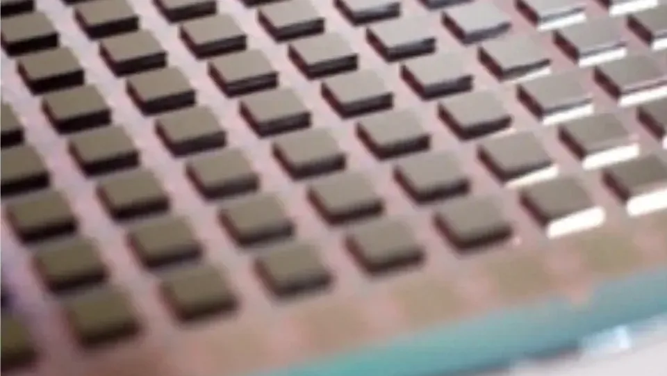
- Chemical Vapor Deposition (CVD) – Silicon precursor for forming high-purity SiO₂ thin films on semiconductor wafers
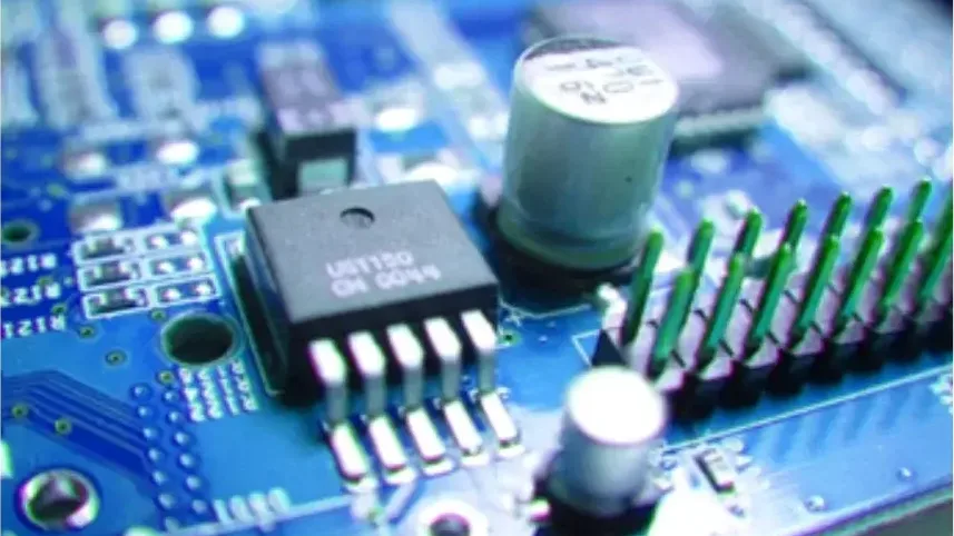
- Semiconductor manufacturing – Essential for producing ICs, transistors, and advanced microelectronic devices
- MEMS and discrete devices – Enables reliable oxide layer formation in Micro-Electro-Mechanical Systems
- Optoelectronics and photonics – Supports fabrication of waveguides, sensors, and transparent dielectric structures
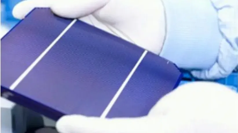
- Solar cell production – Applied in passivation and protective coatings for silicon-based photovoltaic devices
Features
Key Features
TEOS offers exceptional purity, film uniformity, and process control for critical thin-film applications in electronics and photonics.
- Ultra-high purity – Minimizes contamination risk in cleanroom-grade semiconductor environments
- Stable volatility and reactivity – Ideal for controlled CVD processing and uniform SiO₂ film growth
- Versatile applications – Supports industries from semiconductors and solar to optics and specialty coatings
- Excellent compatibility – Works with advanced etching and deposition systems in modern microfabrication
- Reliable global supply – Backed by NAGASE’s logistics network and robust quality assurance
Product Specification
| Item | Grade/99.9999%(6N) | Item | Grade/99.9999%(6N) |
|---|---|---|---|
| Spec value/ppb | Spec value/ppb | ||
| Al | <100 | Mo | <5 |
| As | <50 | Na | <100 |
| Ag | <10 | Ni | <20 |
| Au | <10 | Pb | <20 |
| Ba | <10 | Sb | <20 |
| Bi | <10 | Sn | <50 |
| Ca | <100 | Sr | <5 |
| Cd | <5 | Ti | <10 |
| Co | <5 | Zn | <30 |
| Cr | <10 | Ga | <100 |
| Cu | <15 | Ge | <100 |
| Fe | <100 | Pd | <100 |
| Hg | <10 | Se | <100 |
| In | <5 | Te | <100 |
| K | <100 | V | <100 |
| Li | <10 | B | <100 |
| Mg | <100 | Si | <500 |
| Mn | <20 | S | <200 |
| Product | 9N | ||
|---|---|---|---|
| Purity (based on metals analyzed), min | 99.9999999% | ||
| (Al)max | 0.1 ppb | (Pb)max | 0.1 ppb |
| (Ag)max | 0.1 ppb | (Pd)max | 0.05 ppb |
| (As) max | 0.1 ppb | (Pt)max | 0.05 ppb |
| (Au)max | 0.1 ppb | (Rb)max | 0.05 ppb |
| (B)max | 0.5 ppb | (Re)max | 0.05 ppb |
| (Ba) max | 0.1 ppb | (Rh)max | 0.05 ppb |
| (Be)max | 0.05 ppb | (Sb)max | 0.05 ppb |
| (Bi)max | 0.05 ppb | (Sn)max | 0.05 ppb |
| (Ca)max | 0.2 ppb | (Sr)max | 0.05 ppb |
| (Cd)max | 0.05 ppb | (Ta)max | 0.05 ppb |
| (Ce)max | 0.05 ppb | (Th) max | 0.05 ppb |
| (Co)max | 0.1 ppb | (Ti)max | 0.05 ppb |
| (Cu)max | 0.1 ppb | (Tl)max | 0.05 ppb |
| (Cr)max | 0.1 ppb | (U)max | 0.05 ppb |
| (Fe)max | 0.2 ppb | (V)max | 0.05 ppb |
| (Ga)max | 0.05 ppb | (W)max | 0.05 ppb |
| (Ge)max | 0.05 ppb | (Zn)max | 0.1 ppb |
| (Hf)max | 0.05 ppb | (Zr)max | 0.05 ppb |
| (Hg)max | 0.05 ppb | Cl- max | 50 ppb |
| (In)max | 0.05 ppb | Water max | 5 ppm |
| (Ir)max | 0.05 ppb | Ethanol max | 3 ppm |
| (K)max | 0.2 ppb | Parricles ≥0.1µm max | 50 p/ml |
| (Li)max | 0.05 ppb | Parricles ≥0.2µm max | 10 p/ml |
| (Mg)max | 0.1 ppb | Parricles ≥0.3µm max | 7 p/ml |
| (Mn)max | 0.1 ppb | Parricles ≥0.5µm max | 5 p/ml |
| (Mo)max | 0.05 ppb | Parricles ≥1.0µm max | 1p/ml |
| (Na)max | 0.1 ppb | Assay min | 99.99% |
| (Nb)max | 0.1 ppb | Chroma max | 10APHA |
| (Ni)max | 0.2 ppb | Shelf life | 24 months |
Packaging Size
Container: Stainless Steel Cylinder.
Packaging: Stainless Steel Cabinet.
Fill volume: 2 gallons,5 gallons (19 L),10 gallons, 200 L.
Frequently Asked Questions about Tetraethyl Orthosilicate
What is TEOS used for?
TEOS is primarily used as a silicon precursor in CVD processes to form high-purity silicon dioxide (SiO₂) films on semiconductor wafers and optical substrates.
Why is TEOS important in semiconductor manufacturing?
Its high purity and stable reactivity enable the formation of uniform dielectric layers with low contamination, making it essential for integrated circuits, transistors, and MEMS devices.
What are the advantages of using TEOS in CVD processes?
TEOS offers controlled volatility and excellent compatibility with modern deposition systems, resulting in precise film thickness, good step coverage, and low defect density.
Is TEOS suitable for cleanroom environments?
Yes, ultra-high purity TEOS is specifically tailored for use in cleanroom-grade semiconductor and photonics fabrication, with strict control of metallic and organic impurities.
Related Products
Trimethylaluminum (TMA)
Ultra-high purity metal-organic precursor for ALD and MOCVD. Enables precise deposition of Al₂O₃ and compound semiconductors in photovoltaic and microelectronic industries.

Trimethyl Phosphite (TMP)
High-purity phosphorus precursor for PSG and BPSG layer formation. Enables controlled doping and dielectric deposition in advanced semiconductor manufacturing.

Trimethyl Phosphate (TMPO)
High-purity phosphorus ester for PSG and BPSG deposition. Enables precise dielectric layering in wafer fabrication and microelectronics production.
Trimethyl Borate (TMB)
High-purity boron compound for advanced BPSG deposition. Enables clean doping and dielectric layering in wafer processing and MEMS production.
Triethyl Phosphate (TEPO)
High-purity phosphorus ester for PSG & BPSG deposition. Enables precise dielectric layering in advanced semiconductor manufacturing.

Triethyl Borate (TEB)
High-purity boron ester for advanced chemical applications. Nagase supplies triethyl borate (TEB) used in organic synthesis, cross-coupling reactions, and specialty solvent systems where boron precision is essential.

Trans-1,2-Dichloroethylene (DCE)
High-purity solvent for efficient surface treatment. Nagase delivers trans-1,2-dichloroethylene (DCE) used in polymer production, metal degreasing, and electronics cleaning where performance and purity are critical.
Red Phosphorus
High-purity phosphorus for safety and innovation. Nagase delivers red phosphorus in electronic and industrial grades for flame retardants, semiconductor doping, and specialized materials.
Phosphorus Pentoxide
Powerful dehydration meets phosphorus chemistry. Nagase supplies high-purity P₂O₅ for use in electronics, fine chemical synthesis, and phosphorus-based compound production.

Phosphorus Oxychloride (POCl3)
Reliable reactivity for high-tech manufacturing. Nagase offers POCl₃ in electronic and industrial grades for diffusion doping, phosphorylation reactions, and advanced chemical processes.
